

PSDP group focuses on the development of advanced power devices based on Si and wide bandgap materials (WBG). WBG materials that are researched by the PSDP group includes SiC, GaN and GaO. Both vertical and lateral power devices are being developed. The PSDP group is especially interested in developing medium voltage power switches and rectifiers. The packaging research focuses on how to achieve high temperature operation (>200oC), how to minimize power loop and driving loop parasitic inductance and how to achieve high power density through 3D packaging of system in package (SIP) integration of power devices and passive components.
PSDP Related

Facility
PSDP provides a plenty of equipment featuring curve tracer, probe station, die attach, DBC etching, wire bonding, ultrasonic washer, and 3D printer.

Research Highlight
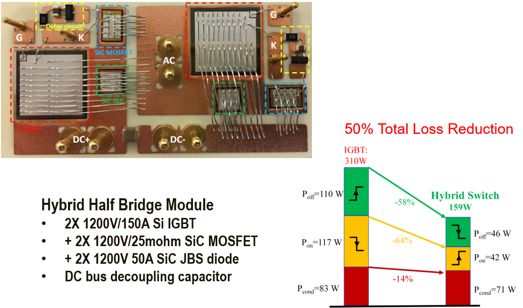
PSDP performs the world-class packaging activity, including integrated gate driver module, 3D package, hybrid power module, and high voltage cascode switch.
PSDP Contact
- Location:
-
Microelectronics Research Center
J.J. Pickle Research Campus
Room 2.402, Bldg. #160, 10100 Burnet Rd
Austin, Texas 78758
- Address:
-
Microelectronics Research Center
J.J. Pickle Research Campus
Bldg. #160, 10100 Burnet Rd
Austin, Texas 78758
- Email: